
Advanced Packaging

Wafer-Level
• 2D & 3D Wafer Inspection System
• Silicon Photonics Probing and Test
• X-Ray 3D Inspection

Die-Level
• Chiplet and Die Testing

Panel-Level
• Substrate and Panel Level Testing

System-Level
• HPC Burn-In
• ATC System-Level Test
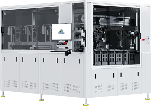
ZANX Series
2D + 3D Wafer Inspection
- Macro & Micro 2D + 3D surface inspection
- Detection sensitivity down to 0.5um
- Bright Field (BF) / Dark Field (DF) optical metrology
- Auto-focus with multi-magnification
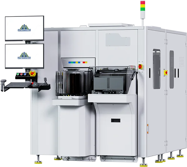
LUMON Series
Silicon Photonics (SiPh) Wafer Probing
- Single & dual-sided wafer probing
- Multi-mode test support (E/O, O/E, O/O, E/E)
- Sub-micron optical alignment
- Low-loss measurement alignment
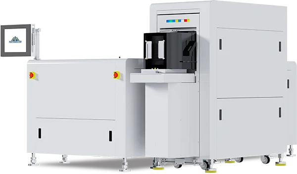
SINAR
X-Ray 3D Inspection
- 3D computed laminography & 2D X-Ray
- High speed imaging with 100nm resolution
- AI-Powered Advanced Metrology
- TSV, TGV, micro-bump and RDL inspection
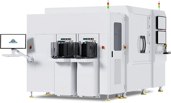
AERO-20
Chiplet & Die Testing
- High pin count support for large SoC and HPC dies
- Hard-docking & optical stack integration
- Tri-tempertaure with Active Thermal Control
- Micron-level pin-to-pad alignment
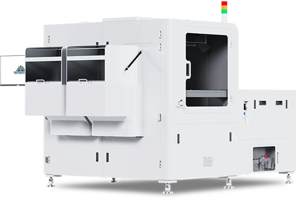
BAYAN
Substrate and Panel Level Testing
- Double side parallel probing
- >40k pin count (top and bottom)
- Supports IVR, LCR and JTAG tests
- Micron level alignment
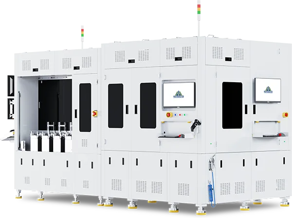
PINTAR
HPC Burn In
- More than 2000W device / 8000W per BIB slot
- 16 burn-in-board (BIB) slots
- Active Thermal Control liquid cooling
- Up to 256 vector I/O
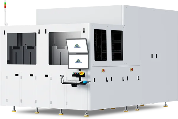
MASON
ATC System-Level Test
- 6 or 12 parallel test sides
- Closed-loop Active Thermal Control
- 300kgf contacr force
- Broad testing conditions: -40 to 150