


PENANG, MALAYSIA (August 2026) – The semiconductor industry is undergoing a fundamental transformation. As the demand for artificial intelligence (AI), high-performance computing (HPC), data centres, autonomous systems, and next-generation consumer electronics continues to accelerate, conventional semiconductor alone is no longer sufficient to deliver the performance, power efficiency, and integration required by modern applications.
Innovation is increasingly driven by how chips are packaged, interconnected, tested, and qualified.
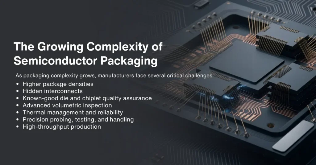
The Growing Complexity of Semiconductor Packaging
Modern semiconductor chips are becoming increasingly heterogeneous. Instead of relying on a single chip, next-generation products often integrate multiple components within a single package to optimise performance.
Supporting the Advanced Packaging Ecosystem
Pentamaster’s advanced packaging solutions are designed to support manufacturers across the entire packaging journey, delivering solutions for inspection, testing, burn-in, characterisation, and handling at various levels of integration.
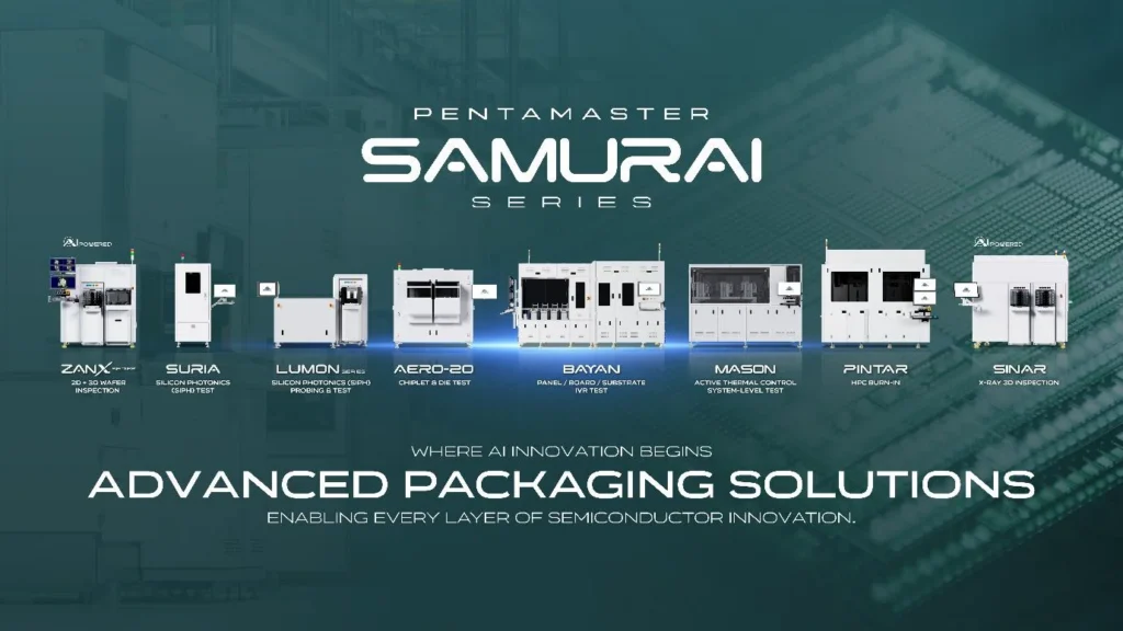
Our capabilities cover:
Wafer-Level
2D + 3D Wafer Inspection
3D X-Ray Inspection
Silicon Photonics (SiPh) Wafer Probing and Test
Die-Level
Die Level & Chiplet Prober
System-Level
HPC Burn-in
ATC System-Level Test
Panel-Level
Substrate and Panel Level Testing
In the coming months, we will take a closer look at the technologies and solutions that support advanced packaging at every level, exploring how manufacturers can address evolving challenges in inspection, testing, validation, and reliability.
Stay connected as we continue to share insights about advancements that shapes the future of semiconductor packaging and manufacturing.